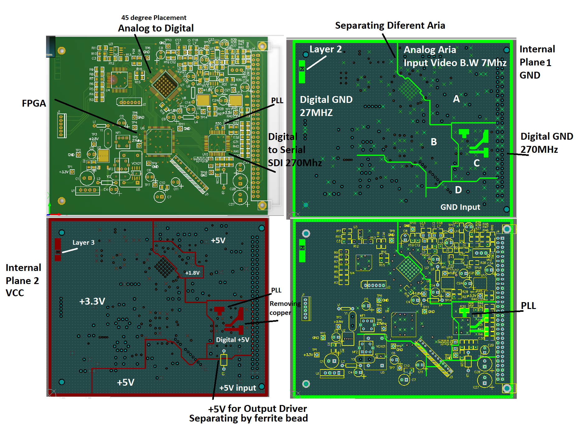
Designing #PCB of #Analog to #Digital #board could be a challenging project for several advanced #PCB_designers. I designed PCB of this analog #video to serial #270MHz (#SDI) for #broadcasting proposes.
The first challenge of this kind of project is the #routing of #GND. The layers of PCB should be, minimum, #four_layers, and the layer under the placement side is #ground (GND). In the internal plane, the ground usually is separated into different sides of analog and digital. In my design, I divided the ground into three main parts A, B, and C. At first is the analog area, A, connected to the main ground from the front side of board. The second is digital ground, B, and the signal is mainly #27Mhz and connected to the main ground from the backside. The third side is under a 270MHz parts.
As a result, in this kind of project, the ground should be separated from each other and connecting them in far point.
I will say more #tips from this project.
@PCBandTIPs
www.pcbdesign.ir
www.pcbtips.com
#PCBTIPs
I am ready to do your #PCB_project soon and professionally!
My WhatsApp: +1 (780) 437 1608
Cell phone: +1 (780) 437 1608
Telegram: https://t.com/PCBandTIPs
Ali Padasha
۹۹/۰۱/۱۶
ارسال نظر آزاد است، اما اگر قبلا در بیان ثبت نام کرده اید می توانید ابتدا وارد شوید.

