The engineers at ExpressPCB have assembled a few general rules-of-thumb that can help beginners design their first circuit board. These tips are not specific to using our CAD software, but instead, provide an overview to help explain how to position the components on the board and how to wire them together.
Placing Components
Generally, it is best to place parts only on the top side of the board.
Continue on Link below:
http://pcbdesign.ir/1398/04/12/Tips-for-Designing-PCBs
When placing components, make sure that the snap-to-grid is turned on. Usually, a value of 0.050″ for the snap grid is best for this job.
First place all the components that need to be in specific locations. This includes connectors, switches, LEDs, mounting holes, heat sinks or any other item that mounts to an external location.
Give careful thought when placing components to minimize trace lengths. Put parts next to each other that connect to each other. Doing a good job here will make laying the traces much easier.
Arrange ICs in only one or two orientations: up or down, and, right or left. Align each IC so that pin one is in the same place for each orientation, usually on the top or left sides.
Position polarized parts (i.e. diodes, and electrolytic caps) with the positive leads all having the same orientation. Also, use a square pad to mark the positive leads of these components.
You will save a lot of time by leaving generous space between ICs for traces. Frequently the beginner runs out of the room when routing traces. Leave 0.350″ – 0.500″ between ICs, for large ICs allow even more.
Parts not found in the component library can be made by placing a series of individual pads and then grouping them together. Place one pad for each lead of the component. It is very important to measure the pin spacing and pin diameters as accurately as possible. Typically, dial or digital calipers are used for this job.
After placing all the components, print out a copy of the layout. Place each component on top of the layout. Check to ensure that you have allowed enough space for every part to rest without touching each other.
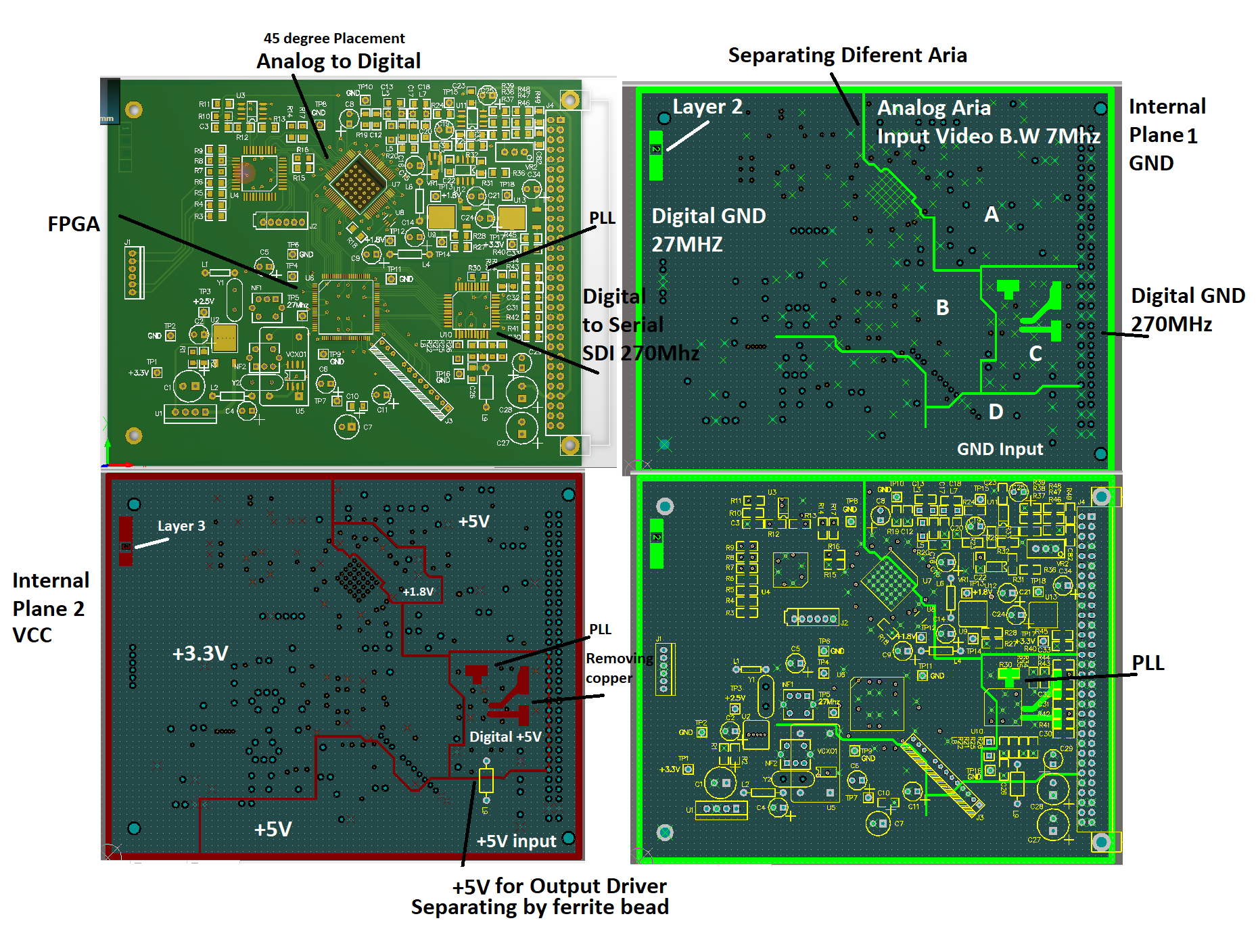
Placing Power and Ground Traces
After the components are placed, the next step is to lay the power and ground traces. It is essential when working with ICs to have solid power and ground lines, using wide traces that connect to common rails for each supply. It is very important to avoid snaking or daisy chaining the power lines from part-to-part.
One common configuration is shown below. The bottom layer of the PC board includes a “filled” ground plane. Large traces feeding on a single rail are used for the positive supply.
Placing Signal Traces
When placing traces, it is always a good practice to make them as short and direct as possible.
Use vias (also called feed-through holes) to move signals from one layer to the other. A via is a pad with a plated-through hole.
Generally, the best strategy is to lay out a board with vertical traces on one side and horizontal traces on the other. Add via were needed to connect a horizontal trace to a vertical trace on the opposite side.
A good trace width for low current digital and analog signals is 0.010″.
Traces that carry significant current should be wider than signal traces. The table below gives rough guidelines of how wide to make a trace for a given amount of current.
0.010″ 0.3 Amps
0.015″ 0.4 Amps
0.020″ 0.7 Amps
0.025″ 1.0 Amps
0.050″ 2.0 Amps
0.100″ 4.0 Amps
0.150″ 6.0 Amps
When placing a trace, it is very important to think about the space between the trace and any adjacent traces or pads. You want to make sure that there is a minimum gap of 0.007″ between items, 0.010″ is better. Leaving less blank space runs the risk of a short developing in the board manufacturing process. It is also necessary to leave larger gaps when working with high voltage.
When routing traces, it is best to have the snap-to-grid turned on. Setting the snap grid spacing to 0.050″ often works well. Changing to a value of 0.025″ can be helpful when trying to work as densely as possible. Turning off the snap feature may be necessary when connecting to parts that have unusual pin spacing.
It is a common practice to restrict the direction that traces run to horizontal, vertical, or 45-degree angles.
When placing narrow traces, 0.012″ or less, avoid sharp right angle turns. The problem here is that in the board manufacturing process, the outside corner can be etched a little more narrow. The solution is to use two 45 degree bends with a short leg in between.
It is a good idea to place text on the top layer of your board, such as a product or company name. Text on the top layer can be helpful to ensure that there is no confusion as to which layer is which when the board is manufactured.
Checking Your Work
After all the traces are placed, it is best to double check the routing of every signal to verify that nothing is missing or incorrectly wired. Do this by running through your schematic, one wire at a time. Carefully follow the path of each trace on your PC layout to verify that it is the same as on your schematic. After each trace is confirmed, mark that signal on the schematic with a yellow highlighter.
Inspect your layout, both top, and bottom, to ensure that the gap between every item (pad to pad, pad to trace, trace to trace) is 0.007″ or greater. Use the Pad Information tool to determine the diameters of pads that make up a component.
Check for missing vias. ExpressPCB will automatically insert a via when changing layers as a series of traces are placed. Users often forget that via are not automatically inserted otherwise. For example, when beginning a new trace, a via is never inserted. An easy way to check for missing via is to first print the top layer, then print the bottom. Visually inspect each side for traces that don’t connect to anything. When a missing via is found, insert one. Do this by clicking on the Pad in the side toolbar; select a via (0.056″ round via is often a good choice) from the drop-down list box, and click on the layout where the via is missing.
Check for traces that cross each other. This is easily done by inspecting a printout of each layer.
Metal components such as heat sinks, crystals, switches, batteries, and connectors can cause shorts if they are placed over traces on the top layer. Inspect for these shorts by placing all the metal components on a printout of the top layer. Then look for traces that run below the metal components.
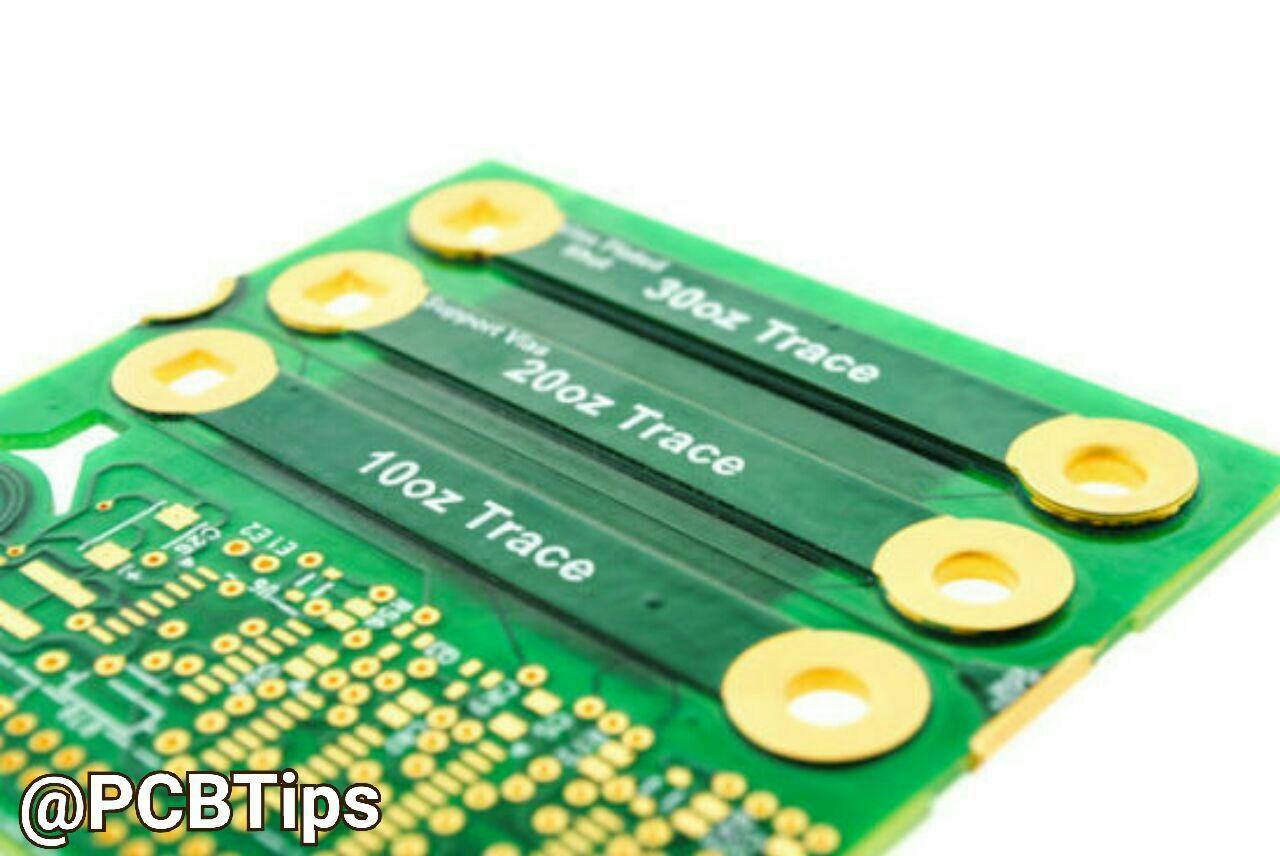 برای بیان قطر مس برد PCB از واحد oz یا اونس استفاده می کنند.